Suppor
Suppor
Package refers to the circuit pins on the silicon chip, which are connected to external connectors with wires in order to connect with other devices. Package type refers to the shell for mounting semiconductor integrated circuit chips. It not only plays the role of installing, fixing, sealing, protecting the chip and enhancing the electric heating performance, etc., but also connects to the pins of the package shell through the contacts on the chip, and these pins are in turn through the wires on the printed circuit board Connect with other devices, so as to realize the connection between internal chip and external circuit.
An important indicator of whether a chip packaging technology is advanced or not is the ratio of chip area to package area. The closer this ratio is to 1, the better. Main considerations when packaging:
1. The ratio of the chip area to the package area is as close to 1: 1 as possible to improve the packaging efficiency
2. The pins should be as short as possible to reduce the delay, and the distance between the pins should be as far as possible to ensure mutual interference and improve performance
3.
Based on heat dissipation requirements, the thinner the package, the better.
Packages are
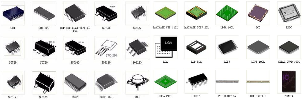
mainly divided into DIP dual in-line and SMD chip packages.
In terms of structure, the package experienced the earliest transistor TO (such
as TO-89, TO92) packaging and developed to a dual in-line package. Subsequently,
PHILIP developed a small SOP package. Later, SOJ (J type) was gradually derived.
(Pin small outline package), TSOP (thin small outline
package), VSOP (very small outline package), SSOP (downsized SOP), TSSOP (thin
reduced size SOP), SOT (small outline transistor), SOIC (small outline
Integrated circuits) and so on. In terms of
material and media, including metals, ceramics, plastics, and plastics, many
circuits that require high-intensity working conditions such as military and
aerospace still have a large number of metal packages.
The
encapsulation has gone through the following development processes:
Structural aspects: TO-> DIP-> PLCC-> QFP-> BGA-> CSP
Material: metal, ceramic-> ceramic, plastic-> plastic
Pin shape: long lead straight insertion-> short lead or
leadless mounting-> spherical bump
Second, the specific
package
1.SOP / SOIC package
SOP is the abbreviation of English Small Outline Package, that is, small outline
package. SOP packaging technology was successfully developed by Philip from 1968
to 1969. Later, SOJ (J-pin small outline package), TSOP (thin small outline
package), VSOP (very small outline package), and SSOP (downsizing SOP), TSSOP
(Thin Reduced SOP), SOT (Small Outline Transistor), SOIC (Small Outline
Integrated Circuit), etc.
2.DIP package
DIP is the abbreviation of English Double In-line Package, that is, dual in-line
package. One of the plug-in packages, the pins are drawn from both sides of the
package, and the package materials are plastic and ceramic. DIP is the most
popular plug-in package, and its applications include standard logic ICs, memory
LSIs, and microcomputer circuits.
3, PLCC package
PLCC is the abbreviation of Plastic Leaded Chip Carrier in English, that is,
plastic J-lead chip package. PLCC packaging method, the shape is square, 32-pin
package, there are pins around, the size is much smaller than the DIP package.
The PLCC package is suitable for mounting and wiring on the PCB using SMT
surface mounting technology, and has the advantages of small size and high
reliability.
4, TQFP package
TQFP is the abbreviation of English thin quad flat package, which is a thin
plastic package with four corner flat packages. The four-sided flat package (TQFP)
process can effectively use space, thereby reducing the requirements on the size
of the printed circuit board. Due to the reduced height and volume, this
packaging process is well-suited for space-critical applications such as PCMCIA
cards and network devices. Almost all ALTERA CPLD / FPGAs are available in TQFP
packages.
5. PQFP package
PQFP is the abbreviation of English Plastic Quad Flat Package, which is a
plastic four-corner flat package. The distance between the pins of the PQFP
package is very small, and the pins are very thin. Generally, large-scale or
ultra-large-scale integrated circuits use this package, and the number of pins
is generally more than 100.
6. TSOP package
TSOP is the abbreviation of English Thin Small Outline Package, that is, thin
small size package. A typical feature of TSOP memory packaging technology is to
make pins around the packaged chip. TSOP is suitable for mounting wiring on PCBs
(printed circuit boards) using SMT technology (surface mount technology). When
the TSOP package dimensions are small, the parasitic parameters (when the
current changes greatly, causing output voltage disturbances) are reduced, which
is suitable for high-frequency applications. It is easy to operate and has high
reliability.
7. BGA package
BGA is the abbreviation of English Ball Grid Array Package, that is, ball grid
array package. In the 20's and 90s, with the advancement of technology, the chip
integration continued to increase, the number of I / O pins increased sharply,
power consumption also increased, and the requirements for integrated circuit
packaging became stricter. In order to meet the needs of development, BGA
packages have begun to be used in production.
Please tell us your purchase demands
About Delsheng


E-MAIL: kylechan@drsic.com